Article: “The Rise of GaN-Based Power Systems—Part II”
The second of a three-part series on The Rise of GaN-Based Power Systems: Technology and Market Overview by Paul Wiener, VP Strategic Marketing, 氮化镓系统 (GaN Systems)
To read the original article in Power Electronics World, click here.
Part 1 of this series exploring gallium nitride (GaN) power devices provided a brief overview of GaN technology fundamentals, describing the growth of GaN power and its main application areas. This second part explores the technical details of applying GaN devices to implement innovative and highly efficient power conversion topologies.
Obtaining the optimum performance advantages of a GaN E-mode (enhancement-mode) high electron mobility transistor (E-HEMT) requires special design considerations, especially under dynamic conditions.
GaN has both lower switching and conduction losses, and its thermal performance provides many high-density power conversion possibilities. Unlike silicon (Si) MOSFETs, a GaN E-HEMT with no body diode has zero reverse recovery losses and exhibits high dv/dt ruggedness. This makes the technology an ideal fit for half-bridge hard switching designs. Meanwhile, both lower gate charge (Qg) and output capacitance (Coss) of GaN HEMTs make the performance of GaN-based soft-switching converters even better.
However, because of fast switching, circuit and layout techniques to minimize noise coupling and the Miller effect are more important than ever. With dv/dt> 100V/ns, GaN E-HEMTS switch faster than Si and silicon carbide (SiC) MOSFETs. GaN has four times faster turn-on and approximately two times faster turn-off time than a state-of-the-art SiC MOSFET with similar RDS(on). As a result, controlling noise coupling from the power to gate drive loop should be the first priority in circuit design. Also, high dv/dt and di/dt combined with low CISS and VG(th) require limiting gate spikes from going above the threshold or maximum rating under the Miller effect for safe operation since any added impedance that modifies the amplifier input impedance can cause problems.
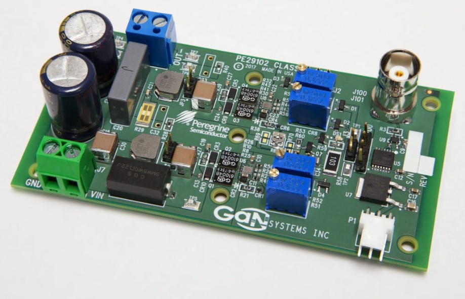
Image 1. The 100 V GaN E-HEMT FB EVB (GS61004B-EVBCD) optimized for Class D amplifiers.
Without proper design considerations, gate ringing or sustained oscillation may occur that can lead to device failure. This is more critical for 650 V hard switching half bridge applications since very high dv/dt spikes could occur at a hard turn-on. A single-ended topology is of less concern for the Miller effect. In addition, the design requirements on dv/dt and di/dt are relaxed for resonant zero voltage switching (ZVS) topology.
To minimize the Miller effect lowering the gate drive impedance (Rg and Lg) is critical, especially at turn-off. The basic rule is the gate needs to be held down as strong as possible with minimum impedance. The Miller effect is more prominent for 650 V-based than 100 V-based designs since the dv/dt is higher for the higher voltage design than in a lower voltage design. In addition, different design techniques are recommended for positive vs. negative dv/dt.
Positive dv/dt
- Prevent false turn-on
- Strong pull-down (low RG/ROL)
- Low LG to avoid ringing
- Use of negative gate bias at turn-off, -2 to -3V, helps
Negative dv/dt
- Occurs at turn-on of the complementary switch in half bridge
- Keep VGS-_pk within -10 V
- Strong pull-down (low RG/ROL) and low LG for lower ringing
- VGS may bounce back >0V (LC ringing), so ensure VGS+_pk< VG(TH) to avoid false turn-on or gate oscillation
GaN E-HEMT speed can be easily controlled by gate resistors. A separate RGfor turn-on and turn-off is recommended. For controlling the Miller effect, an RG(ON)/RG(OFF) ratio ≥ 5 to 10 is recommended.
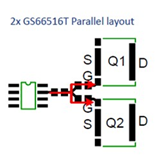
Image 2. Symmetry of dual gate drive in parallel design reduces PCB space.
For more details, please refer to the application guide “Design with GaN Enhancement mode HEMT” [1].
PCB Layout
With their fast switching time, GaN E-HEMTs require the usual layout considerations to avoid gate ringing and oscillation. Suggested best layout practices for gate drives include:
- Physically separating the power loop and the drive loop areas to minimize noise coupling
- Minimizing the pull-down loop by locating the gate driver close to the ground capacitor
- Minimizing the turn-on (pull-up) loop by locating the VDD capacitor close to the driver
- Isolating and avoiding overlap between gate drive and drain copper pad
- Isolating and avoiding overlap from Drain/Source to control grounds
Several low (80-100 V) and high (650 V) voltage half/full bridges and gate driver/controller ICs from different suppliers have been verified to work with GaN E-HEMTs and simplify the implementation of best practices. Image 1 shows the GS61004B-EVBCD with a 60 V half-bridge GaN driver optimized for high frequency applications that include DC/DC conversion and wireless power charging.
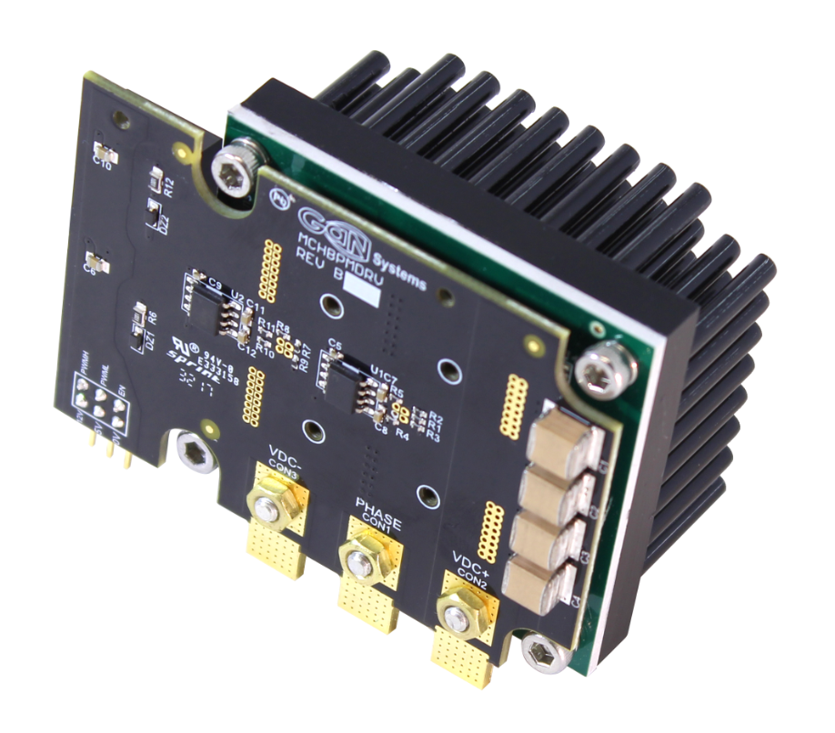
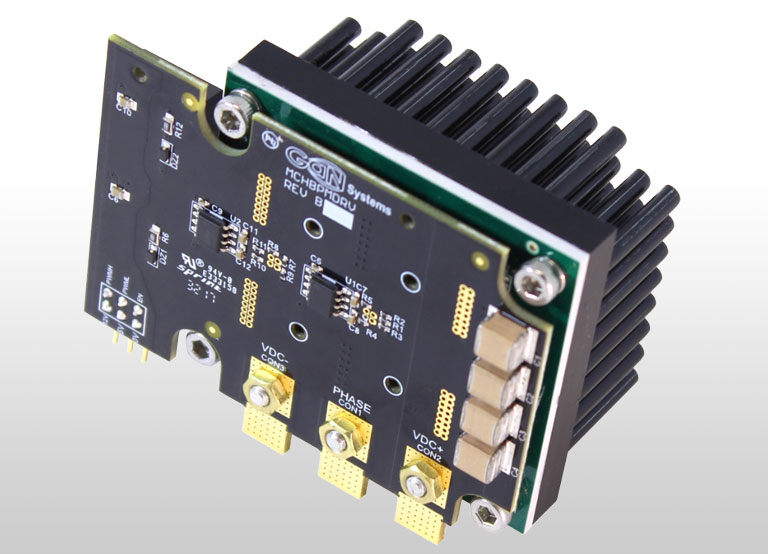
Image 3. An IMS evaluation module integrates a gate driver board and IMS PCB with a heatsink.
Paralleling Techniques for GaN
GaN technology’s RDS(on) and transfer characteristics, including transconductance that decreases with temperature, provide negative feedback to self-balance and compensate devices and overcome circuit mismatches. In addition to reducing the total gate drive loop in paralleling designs, a dual-gate drive makes it easier to have a symmetric gate drive layout and reduce the total layout footprint area.
Image 2 shows the parallel layout for two GS66516T GaNPX® packaged devices. The gate drive requirements for GaN are five to 10 times less than an equivalent Si MOSFET and have 50 times or greater lower gate drive losses at MHz-level switching.
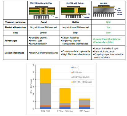
Image 4. Comparison of several design parameters including junction to heatsink thermal resistance (RthJ-HS) for FR4 PCB with cooling vias and FR4 PCB with Cu inlay to an insulated metal substrate (IMS) board. Thermal results are estimated based on the GS66516B GaN E-HEMT.
The IMS module design approach has been used in automotive, industrial, server/datacenter, and consumer applications. Automotive applications include on-board chargers, DC/DC converters, three-phase inverters and high power wireless chargers. For industrial applications, the modules have been used in 3-7 kW photovoltaic inverters as well as energy storage systems (ESS) and motor drives, including variable frequency drives. Servers/datacenters have employed a 3 kW AC/DC power supply. Finally, IMS modules have been used in consumer/residential energy storage systems. In contrast to thermal cooling for surface mount technology (SMT) packages that often use cooling vias or a copper (Cu) inlay, the IMS board provides several advantages as summarized in Image 4.
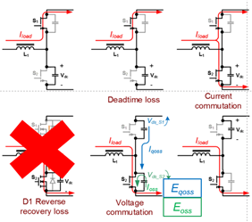
Image 5. Hard switch-on transition and switch commutation principle of a GaN HEMT.
Switching Transient and Loss Analysis of GaN
The hard-switching turn-on transition for GaN HEMTs is shown in Image 5. Compared to Si MOSFETs, the absence of reverse recovery loss means a relatively clean channel current Id waveform.
A capacitive Eqoss loss is part of the hard-switching losses. For GaN HEMTs, the absence of the Qrr makes the Qoss noticeable although the value of the Qoss for GaN HEMTs is still the smallest among both Si and SiC MOSFETs. The Eoss loss is introduced by the capacitance self-discharging current of the switch device itself and Eqoss loss is introduced by the capacitance charging current from the opposite switch device. Image 6 shows the difference between hard switching-on loss distribution in Si MOSFETs vs. GaN E-HEMTs.
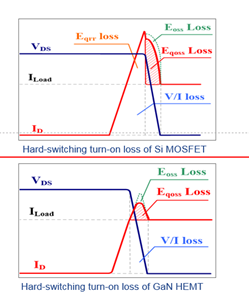
Image 6. No reverse recovery loss and lower capacitive loss mean lower Eon loss for GaN E-HEMTs.
Eon/Eoff Scaling Method for GaN
The Eon of GaN E-HEMTs depends on the junction temperature (Tj). Also, the devices from 氮化镓系统 (GaN Systems) are highly scalable. As a result, an Eon/Eoff scaling method for GaN can be used to obtain the Eon/Eoff at other operating conditions (different Vds, Tj, and Rg), by scaling the data from the initial operating conditions. Image 7 shows the step-by-step Eon/Eoff scaling procedure.
This approach mainly requires three steps for both Eon and Eoff scaling. For Eon, the first step is Rg scaling. Next is the Eqoss calculation and Vds scaling. The third step is Tj scaling.
For Eoff, the first step is Rg and Tj scaling, next is the Eoss calculation, and third is Vds scaling. In this analysis, the initial condition is defined as Vds=400V, Rg_on=10Ω, Rg_off=2Ω, and Tj=25°C. Note that the initial condition can be revised with an accurately measured Eon/Eoff curve.
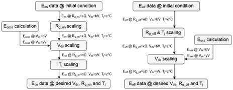
Image 7. Eon/Eoff scaling procedure/algorithm for GaN HEMTs.
Dynamic Rdson
Trapping is a common problem in wide bandgap (WBG) semiconductors like GaN. It impacts the dynamic RDSon (Rdyn) of GaN devices. While Rdyn reduces with higher junction temperatures due to the GaN E-HEMT’s positive temperature coefficient, other factors that affect Rdyn include:
- Bias voltage
- Bias time
- Switching frequency
- Duty cycle
It should be noted that dynamic RDS(on) effects are negligible in steady state operation.
Moving to GaN
With proper design considerations, designing engineers can build power systems that have one-quarter of the power loss, size, and weight of Si-based solutions at a fraction of the cost. This second in a series GaN article, identified and discussed several key product characteristics and circuit aspects toward achieving those results.
Editor’s Note: Part III of this series by 氮化镓系统 (GaN Systems) will discuss topologies based on gallium nitride technology as well as specific applications including wireless power.